
Engineering Reliability: Specialized PCB Design and Development at Relia Test Labs
In the fast-paced world of semiconductor manufacturing and high-tech hardware development, a product is only as strong as its foundation. At Relia Test Labs, we understand that reliability isn’t an afterthought—it’s a fundamental requirement that must be engineered into a product from the very first trace on a PCB.
While many firms offer generic layout services, Relia Test Labs provides a specialized, engineering-driven approach to PCB design. We focus on the high-stress environments where failure isn’t an option, providing turnkey solutions for the most demanding test and production interfaces
Turnkey Design for High-Stress Environments
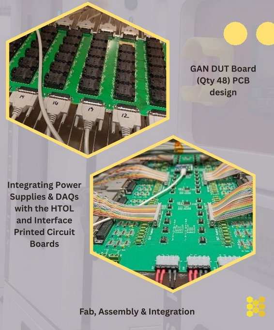
Our core expertise lies in the design and manufacture of specialized test boards that are essential for reliability verification. Whether it is for HAST (Highly Accelerated Stress Test), LTOL (Low Temperature Operating Life), or Burn-in cycles, the boards themselves must withstand the same extreme conditions as the components under test.
We provide full turnkey services including:
- Burn-in Boards: Custom-designed to handle high power levels and I/O counts while maintaining signal integrity at elevated temperatures.
- HAST Boards: Engineered with specialized materials to resist moisture penetration and conductive anodic filament (CAF) growth under high pressure and humidity.
- Load Boards & Probe Cards: High-precision interfaces for wafer-level and chip-level testing.
Material Science and Component Selection
A reliable design is only as good as the materials used. ReliaTest Labs leverages decades of experience in environmental testing to select critical materials—such as high-Tg laminates and specialized solder alloys—that prevent delamination and joint failure during thermal cycling. Our engineers carefully select sockets and connectors that can endure thousands of cycles without degradation, ensuring your test data remains accurate and your downtime remains zero.
Integrating Design for Reliability (DfR)
At Relia Test Labs, our design process is deeply integrated with our Engineering Services. We don’t just “route” a board; we analyze it. During the design phase, we utilize a suite of reliability tools to ensure the long-term viability of the hardware:
- Failure Modes and Effects Analysis (FMEA): Identifying potential failure points in the layout before they reach the prototype stage.
- De-rating Analysis: Ensuring that all components are operating well within their electrical and thermal limits to extend product lifespan.
- Thermal Characterization: Using high-resolution thermography and simulation to identify hot spots that could lead to premature failure.
Relia Test Labs works as a strategic partner throughout the product lifecycle. From the Concept Phase, where we perform reliability gap analysis, to the Manufacturing Phase, where we develop HASS (Highly Accelerated Stress Screening) plans, our PCB design services ensure that your hardware is robust, compliant, and ready for market.
Bridging the Gap from Concept to Production
By following JEDEC, MIL-STD, and ASTM standards, we ensure that every board we design meets the rigorous requirements of the automotive, aerospace, medical, and semiconductor industries.
Ready to strengthen your next design? Whether you need a custom HAST fixture or a high-density burn-in board, Relia Test Labs has the engineering expertise to bring your vision to life with reliability at its core.
Contact our Silicon Valley facility today to discuss your specific PCB design and engineering requirements!